
In the high-stakes world of AI infrastructure, the industry has operated under a singular assumption: flexibility is king. We build general-purpose GPUs because AI models change every week, and we need programmable silicon that can adapt to the next research breakthrough.
But Taalas, the Toronto-based startup thinks that flexibility is exactly what’s holding AI back. According to Taalas team, if we want AI to be as common and cheap as plastic, we have to stop ‘simulating’ intelligence on general-purpose computers and start ‘casting’ it directly into silicon.
The Problem: The ‘Memory Wall’ and the GPU Tax
The current cost of running a Large Language Model (LLM) is driven by a physical bottleneck: the Memory Wall.
Traditional processors (GPUs) are ‘Instruction Set Architecture’ (ISA) based. They separate compute and memory. When you run an inference pass on a model like Llama-3, the chip spends the vast majority of its time and energy shuttling weights from High Bandwidth Memory (HBM) to the processing cores. This ‘data movement tax’ accounts for nearly 90% of the power consumption in modern AI data centers.

Taalas’s solution is radical: eliminate the memory-fetch cycle. By using a proprietary automated design flow, Taalas translates the computational graph of a specific model directly into the physical layout of a chip. In their HC1 (Hardcore 1) chip, the model’s weights and architecture are literally etched into the wiring of the silicon.

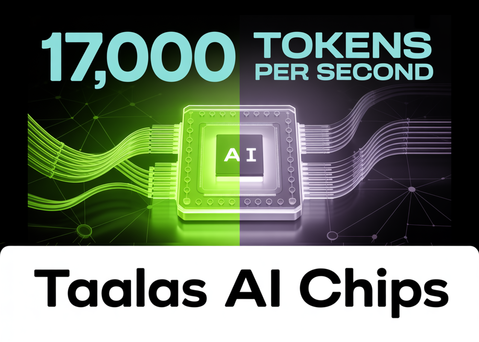
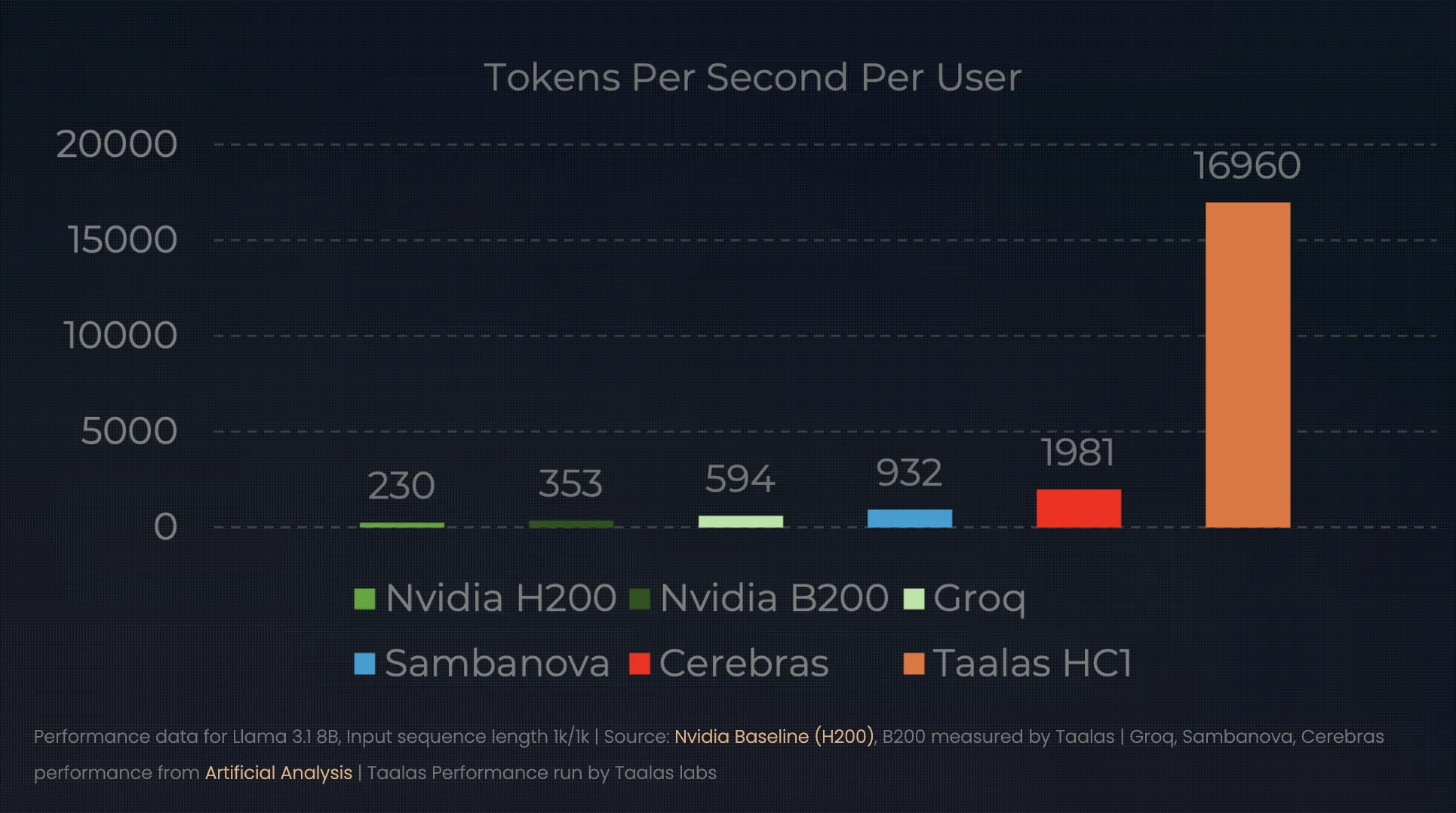
Hardcore Models: 17,000 Tokens Per Second
The results of this ‘direct-to-silicon’ approach redefine the performance ceiling for inference. At their latest unveiling, Taalas demonstrated the HC1 running a Llama 3.1 8B model. While a top-tier NVIDIA H100 might serve a single user at ~150 tokens per second, the HC1 serves a staggering 16,000 to 17,000 tokens per second.
This changes the ‘unit economics’ of AI:
- Performance: A single HC1 chip can outperform a small GPU data center in terms of raw throughput for a specific model.
- Efficiency: Taalas claims a 1000x improvement in efficiency (performance-per-watt and performance-per-dollar) compared to conventional chips.
- Infrastructure: Because the weights are hardwired, there is no need for external HBM or complex liquid cooling systems. A standard air-cooled rack can house ten of these 250W cards, delivering the power of an entire GPU cluster in a single server box.
Breaking the 60-Day Barrier: The Automated Foundry
The obvious ‘catch’ for an AI developer is flexibility. If you hardwire a model into a chip today, what happens when a better model comes out tomorrow? Historically, designing an ASIC (Application-Specific Integrated Circuit) took two years and tens of millions of dollars.
Taalas has solved this through automation. They have built a compiler-like foundry system that takes model weights and generates a chip design in roughly a week. By focusing on a streamlined manufacturing workflow—where they only change the top metal masks of the silicon—they have collapsed the turnaround time from ‘weights-to-silicon’ to just two months.
This allows for a ‘seasonal’ hardware cycle. A company could fine-tune a frontier model in the spring and have thousands of specialized, hyper-efficient inference chips deployed by summer.
The Market Shift: From Shovels to Stamps
This transition marks a pivotal moment in the AI hype cycle. We are moving from the ‘Research & Training’ phase—where GPUs are essential for their flexibility—to the ‘Deployment & Inference’ phase, where cost-per-token is the only metric that matters.
If Taalas succeeds, the AI market will split into two distinct tiers:
Key Takeaways
- The ‘Hardwired’ Paradigm Shift: Taalas is moving from software-defined AI (running models on general-purpose GPUs) to hardware-defined AI. By ‘baking’ a specific model’s weights and architecture directly into the silicon, they eliminate the need for traditional instruction-set overhead, effectively making the model the processor itself.
- Death of the Memory Wall: Traditional AI hardware wastes ~90% of its energy moving data between memory and compute. Taalas’s HC1 (Hardcore 1) chip eliminates the “Memory Wall” by physically wiring the model parameters into the chip’s metal layers, removing the need for expensive High Bandwidth Memory (HBM).
- 1000x Efficiency Leap: By stripping away the ‘programmability tax’, Taalas claims a 1,000x improvement in performance-per-watt and performance-per-dollar. In practice, this means an HC1 can hit 17,000 tokens per second on a Llama 3.1 8B model—massively outperforming a standard GPU rack while using far less power.
- Automated ‘Direct-to-Silicon’ Foundry: To solve the problem of model obsolescence, Taalas uses a proprietary automated design flow. This reduces the time to create a custom AI chip from years to just weeks, allowing companies to ‘print’ their fine-tuned models into silicon on a seasonal basis.
- The Commodity AI Future: This technology signals a shift from ‘Cloud-First’ to ‘Device-Native’ AI. As inference becomes a cheap, hardwired commodity, AI will move off centralized servers and into local, low-power hardware—ranging from smartphones to industrial sensors—with zero latency and no subscription costs.
Check out the Technical details. Also, feel free to follow us on Twitter and don’t forget to join our 100k+ ML SubReddit and Subscribe to our Newsletter. Wait! are you on telegram? now you can join us on telegram as well.